Dielectric materials are commonly referred to as electrical insulators. As very large scale integrated (VLSI) microelectronics technology has developed in this millennium, the need for specialized materials with (i) low-K dielectric constants, as well as (ii) high-K dielectric constants, within such circuits has become critical.
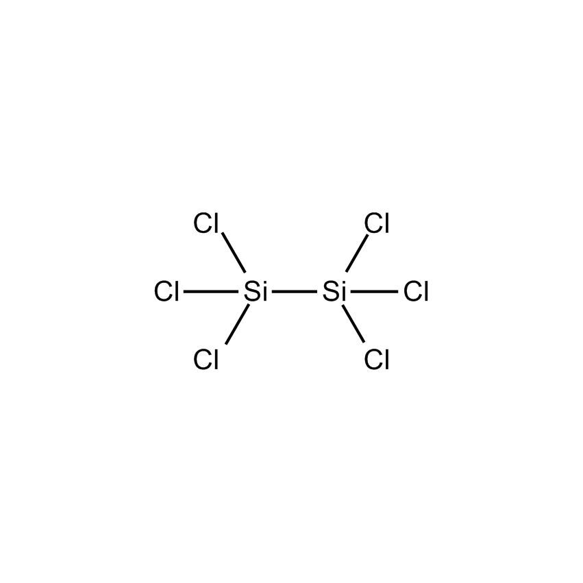
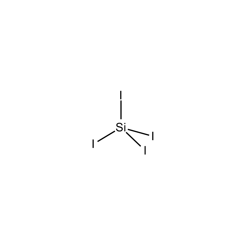
Under the influence of small fields electrons move quite freely through conductors, whereas in insulators or dielectric materials, fields displace electrons only slightly from their equilibrium conditions. The slight displacement of electrons is said to polarize the dielectric. The dielectric constant is related to both induced polarization and permanent dipole. In actual applications, dielectric materials have a wide range of compositions and physical forms (as seen in the examples below). They are conventional insulators as well as precursors or intermediates for structures with precisely controlled dielectric properties.
Continuous improvements of integrated circuit devices to smaller feature sizes and faster speeds have reached a point where the interconnect signal delay, or resistance-capacitance delay, becomes comparable to transistor gate delay. In semiconductors, a low-K dielectric is a material with a small dielectric constant relative to silicon dioxide. Low-K dielectric material allows scaling of microelectronics devices and insulating dielectrics can get closer without charge build up and adverse effects on device performance.
More technologically advanced integrated circuits with smaller feature sizes will require interlayer dielectric materials with lower dielectric constants than current silicon dioxide to prevent electronic crosstalk and also to lower power consumption. As a result, a flurry of activity has occurred in the past years to develop low-K options. Low-K can be achieved by increasing porosity of silicon dioxide or doping of carbon or fluorine. Silsesquioxanes (sometimes given the designation POSS), which can be viewed as a hybrid of silica and organics, have lower K values than SiO2 good thermal stability, and attractive mechanical properties.
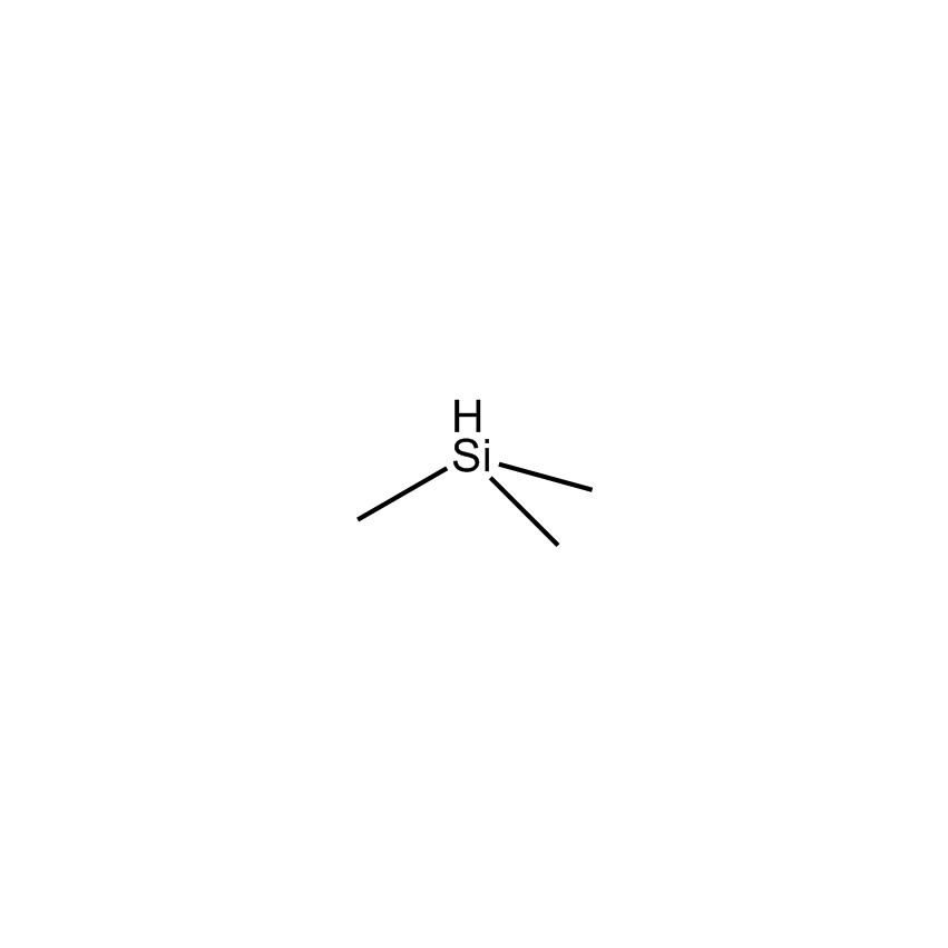
Silsesquioxanes with many Si-H groups, for instance, have a K of ~2.8. Introducing porosity into such silsesquioxanes, [prepared by blending it with a high boiling organic solvent followed by rapid cure and high-temperature elimination of volatiles], can provide K values from 1.5 to 2.5. Similarly, porous methyl silsesquioxanes have been used as low-K materials. The use of chemically modified silsesquioxanes or copolymers that contained an organic spacer or pendant group which can be thermally degraded after cure to generate porosity has also been tried as a low k dielectric material.
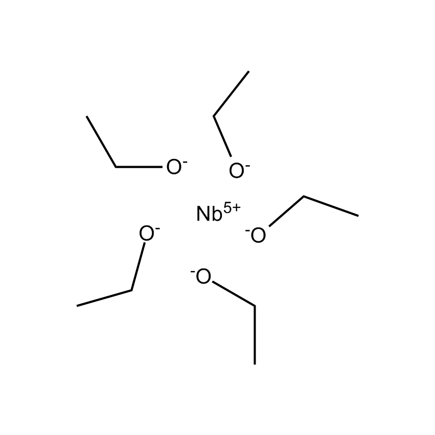
High-performance dielectric materials, known as high-K dielectric constant materials, are also expected to play increasingly important roles in the next generation of electronics and very large scale integrated (VLSI) microelectronics technology. Silica-based ceramic materials, such as silica (SiO2), hafnium silicate (HfSiO4), and zirconium silicate (ZrSiO4), are common interlayer dielectric materials used in high density microelectronic packaging. Barium titanate (BaTiO3) is one of well-known dielectric materials that is also used in a variety of semiconductor devices owing to its high and frequency-independent permittivity with low dielectric loss. Many researchers have attempted to disperse high dielectric, barium titanates and other ceramic oxides, into polymers followed by their fabrication into thin films.
Existing dielectric capacitors have low energy densities, both on a volume and on a mass basis. No current capacitor technology has the combination of energy density, power density, and rate capability desired for portable pulse power systems currently under development or envisioned for the future. Silicon dioxide has been used as a gate oxide material for decades. However, as transistors have decreased in size, the thickness of the silicon dioxide gate dielectric has to be decreased to increase the gate capacitance. The reduced thickness scales below 2nm leads to leakage currents, to unwieldy power consumption, and reduced device reliability. A high-K dielectric material allows increased gate capacitance without the concomitant leakage effects.
The most obvious way to increase the energy density would be to choose dielectric materials with the highest possible breakdown field strength. Many polymers not only have high values of the dielectric breakdown field strength, but also provide the additional advantage of processability. Unfortunately, the dielectric constants for polymers are relatively low. Blending high dielectric inorganic ceramic materials into polymers can lead to higher effective dielectric constants and thus increase the energy density. Importantly, surface modification of BaTiO3 by various organo-phosphonic acids leads to a better dispersion of BaTiO3 particles in the polymer matrix and so to a high effective dielectric constant.
In the field of high-permittivity dielectrics it is highly desirable to have the grains of the ceramic composed of a core of virtually pure BaTiO3 surrounded by a shell where titanium is partially replaced by a different element, like zirconium or niobium. The local gradient gives a distribution of the Curie temperature and, consequently, flatter dielectric temperature characteristics in comparison to pure BaTiO3. These locally inhomogeneous ceramics are usually obtained by mixing a BaTiO3 powder with a second oxide, like ZrO2 or Nb2O5, and then sintering in the presence of a liquid phase.
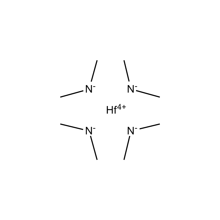
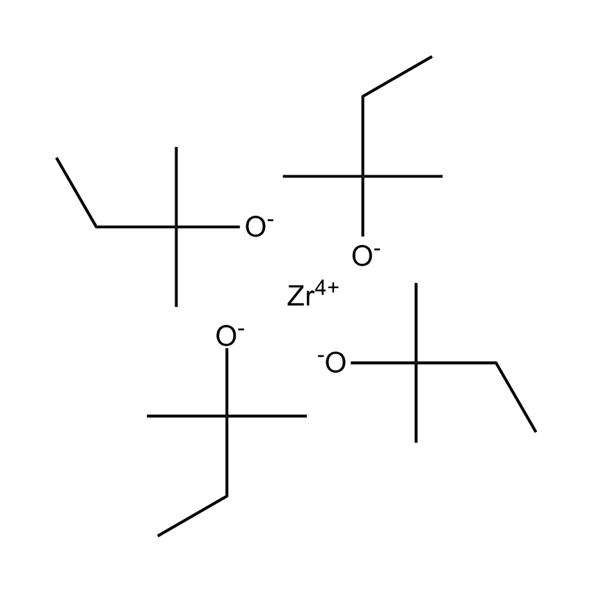
Several materials below are recommended high k precursors and typically deposited using atomic layer deposition (see separate application note).
Uses
Insulators
Conventional insulators in electrical and microelectronic encapsulation
Rectifiers, semiconductors, transducers, capacitors, and transformers
Applications where dielectric properties are controlled for active device architectures

