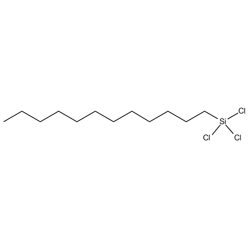
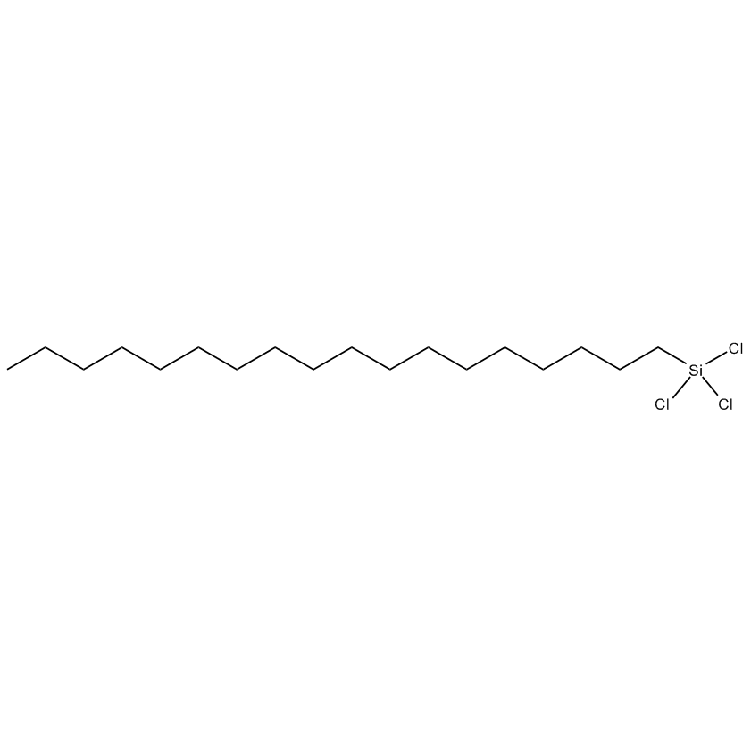
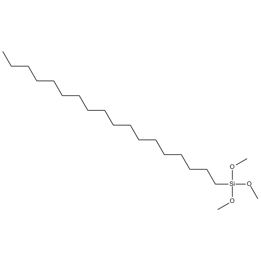
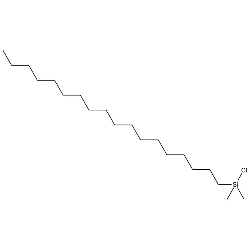
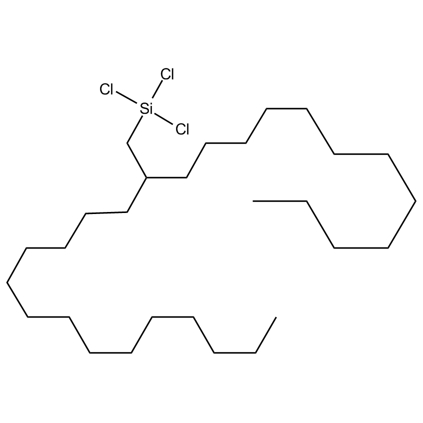
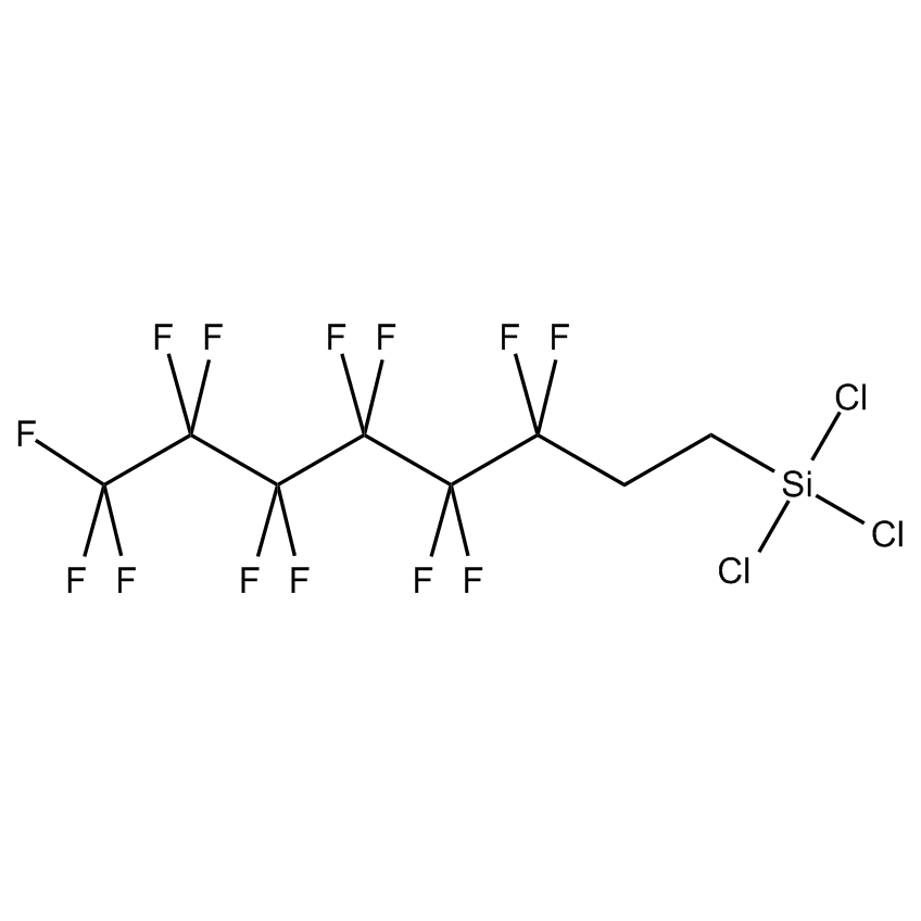
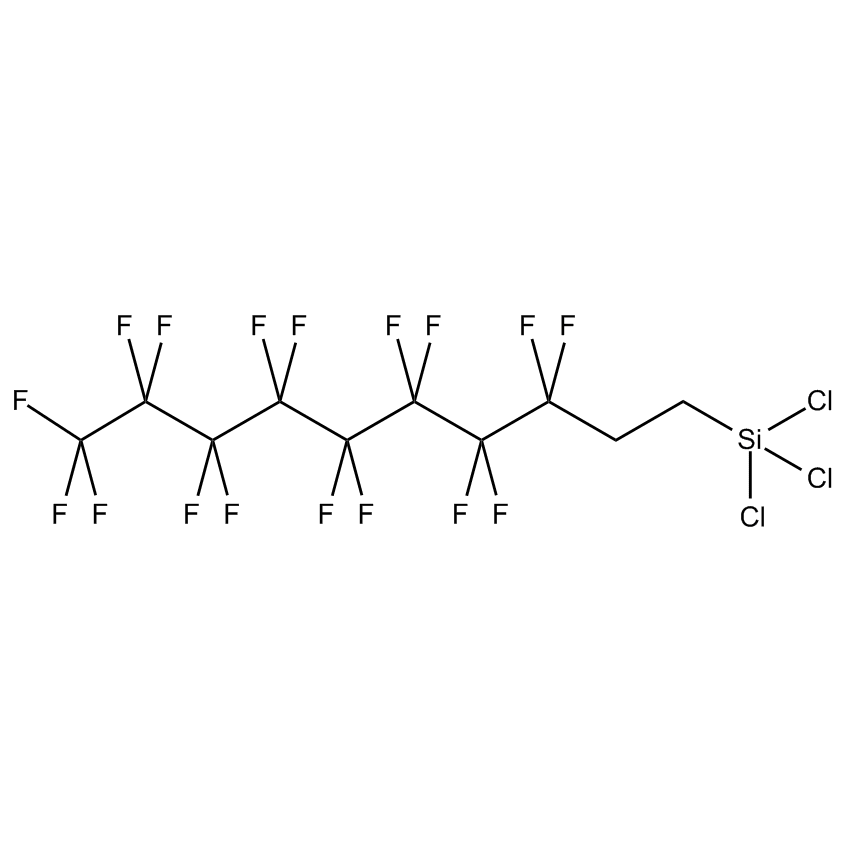
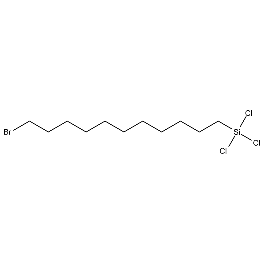
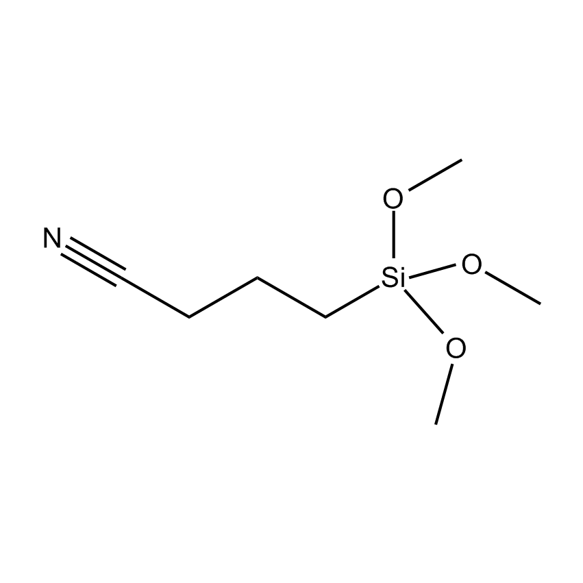
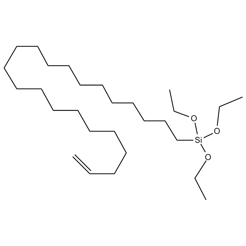
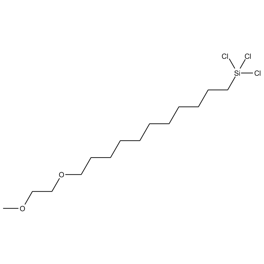
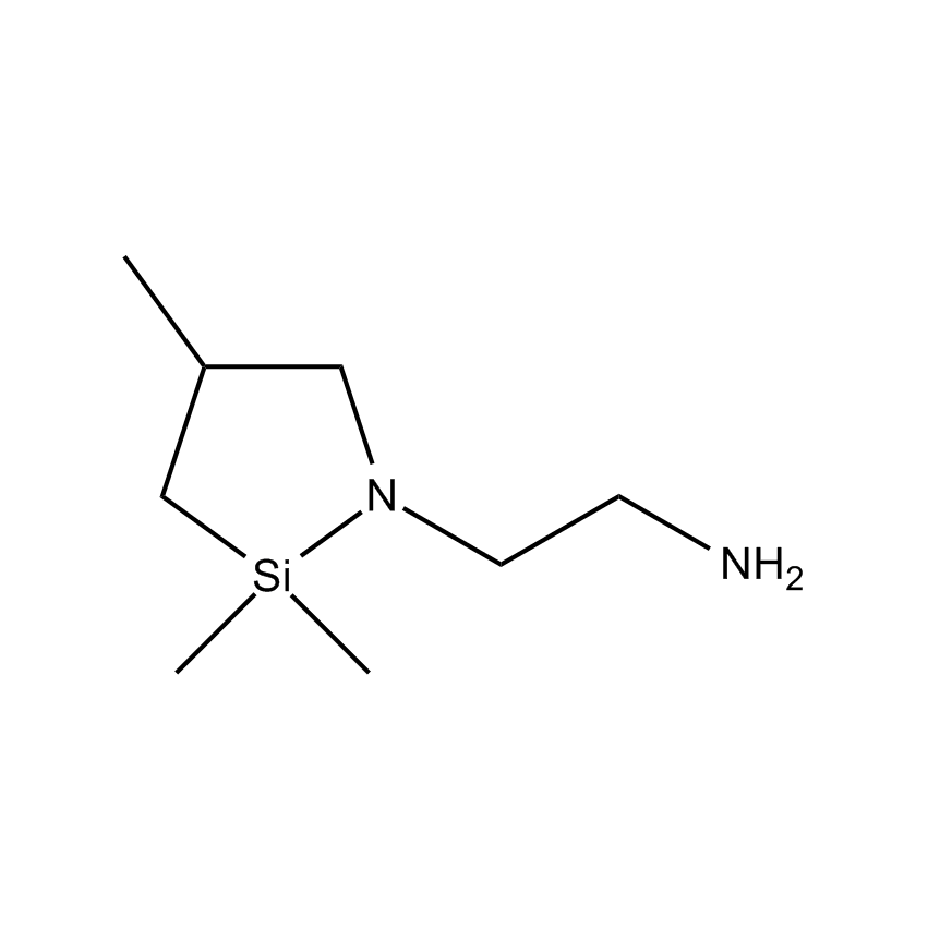
A self-assembled monolayer (SAM) is a one molecule thick layer of material that bonds to a surface in an ordered way as a result of physical or chemical forces during a deposition process. Silanes can form SAMs by solution or vapor phase deposition processes. Most commonly, chlorosilanes or alkoxysilanes are used. Once deposition occurs, a chemical (oxane or Si-O-M) bond forms with the surface rendering a permanent modification of the substrate.
Common long chain alkyl silanes used in the formation of SAMs are simple hydrocarbon, fluoroalkyl and end-group substituted silanes. Silanes with one hydrolysable group maintain interphase structure after deposition by forming a single oxane bond with the substrate. Silanes with three hydrolysable groups form siloxane (silsesquioxane) polymers after deposition, bonding both with each other as well as the substrate. The minimization of water condensation at the substrate can prevent the random aggregation and reaction among the silanes and increase attachment to the substrate. Formation of well-ordered oxane bonds with surface hydroxyl groups depend on the density (or frequency) of a materials surface hydroxyl groups (M-OH), and this varies between different materials, so selecting a silane with the right number of hydrolysable groups is very important.
Self-assembled monolayers are now established as crucial interlayers and electronically active layers in organic electronic devices, such as organic light emitting diodes (OLEDs), organic photovoltaics (OPVs), organic thin film transistors (OTFTs), and nonvolatile memories (NVMs). The use of self-assembling functionalized silanes remains beneficial, due to mainly three advantages compared with common thin film deposition approaches. Molecular self-assembly occurs with surface selectivity, determined by the interaction between the functional anchor group (chloro or alkoxy) of the silane coupling agent and the target surface.
The film thickness of the resulting layers is controlled on the angstrom scale, so that the self-terminating film formation results in only a single molecular layer.
The wide variability in the chemical structure of the silanes produced by Gelest enables different SAM functionalities for devices, ranging from electrical insulation to charge storage to charge transport. The SAM approach can be further expanded by employing several functionalized silanes simultaneously to create mixed SAMs with consequently mixed properties.
The function of SAMs in devices depends not only on the chemical structure of the silane molecules but also on their final arrangement and orientation on the surface. Careful control of silane application has promoted silane applications in micro-contact printing, soft lithography, dip-pen nanolithography, anti-stiction coatings and orientation layers involved in nanofabrication of MEMs, fluidic microassemblies, semiconductor sensors and memory devices. SAMs are used to fine-tune the work functions of inorganic electrodes, thereby minimizing the energy barriers for injection or extraction of charge carriers into or out of an active silane layer. In the field of molecular electronics, the SAM itself (or, in some cases, one or a few molecules) carries the entire device functionality; the interface then essentially becomes the device and the alignment of the molecular energy levels with those of the electrodes defines the overall charge-transport characteristics.
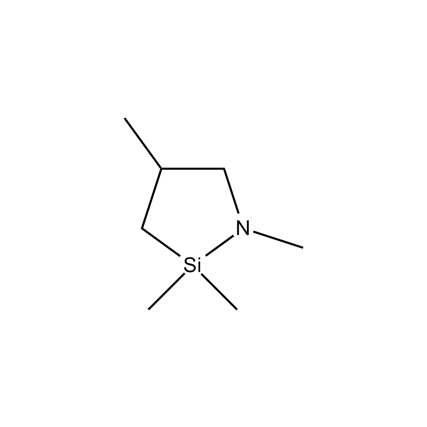
The precise nature of SAMs in molecular electronics has led to the recent vapor deposition of cyclic azasilanes at Gelest. These silanes are applied on surfaces in the absence of either alcohols or water and attach to surface hydroxyl groups directly without generating any other products.
